

New Semiconductor Technology Could Strengthen America’s AI Hardware Industry
The global race for artificial intelligence leadership is driving a new wave of semiconductor innovation. As AI models become larger and computing demands continue to increase, traditional chip manufacturing approaches are facing growing challenges.
To address these challenges, the U.S. Department of Commerce has announced plans to invest up to $140 million in advanced semiconductor packaging research through the CHIPS Research and Development Office.
The proposed funding will support semiconductor equipment manufacturer Multibeam in developing next-generation chip packaging technologies designed to improve performance, efficiency, and scalability for future AI and high-performance computing systems.
Why Advanced Chip Packaging Matters
For decades, semiconductor progress has mainly focused on making transistors smaller and increasing the number of components that can fit onto a single chip.
However, modern AI workloads are creating new demands that traditional chip scaling alone cannot solve.
Large AI systems require:
- Massive computing power
- Faster data movement
- Lower energy consumption
- Higher memory bandwidth
- More efficient hardware integration
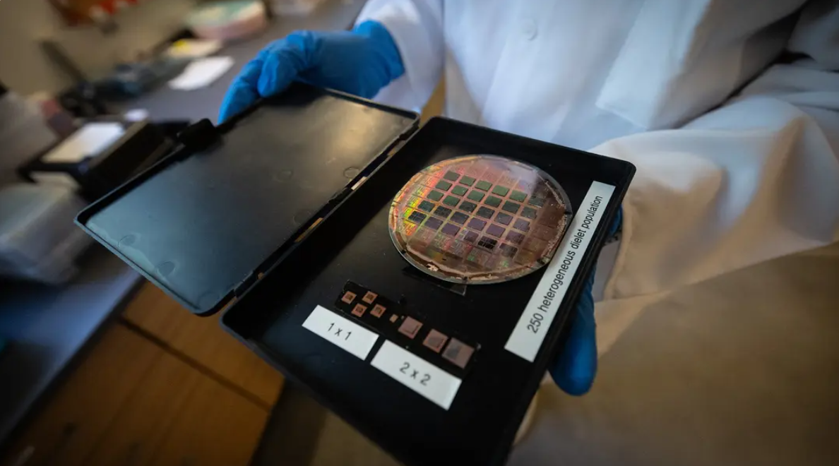
Advanced packaging has emerged as a key technology because it allows multiple smaller chips, known as chiplets, to work together as a single high-performance system.
Instead of creating one extremely large chip, manufacturers can combine multiple specialized components into one package.
The Rise of Chiplet Technology
Chiplets represent a major shift in semiconductor design.
Traditional processors are built as a single large piece of silicon. While this approach has delivered decades of progress, manufacturing extremely large chips has become increasingly expensive and technically difficult.
Chiplet-based designs offer several advantages:
Better Performance
Different chiplets can be optimized for specific tasks, allowing systems to achieve higher performance.
Lower Manufacturing Costs
Smaller chip designs often have better production yields compared with very large chips.
Greater Flexibility
Companies can combine different technologies, such as computing cores, memory systems, and AI accelerators, into customized solutions.
This approach is becoming increasingly important for artificial intelligence, cloud computing, and advanced data centers.
Fine-Pitch Advanced Packaging Technology
The proposed CHIPS funding will support research into fine-pitch advanced packaging process flows.
This technology focuses on connecting multiple semiconductor components with extremely precise alignment.
Smaller connection distances can improve:
- Data transfer speeds
- Energy efficiency
- Overall system performance
For AI applications, where enormous amounts of data must move quickly between processors and memory, these improvements could have significant impact.
Supporting the AI Computing Revolution
Artificial intelligence has created unprecedented demand for powerful computing hardware.
Modern AI systems rely heavily on advanced semiconductor technologies to process billions of calculations efficiently.
Applications benefiting from improved chip packaging include:
- Large language models
- Autonomous vehicles
- Robotics systems
- Scientific simulations
- Cloud AI services
- High-performance computing
As AI continues expanding into more industries, efficient semiconductor infrastructure will become increasingly important.
Strengthening the US Semiconductor Supply Chain
The investment is also part of a broader effort to strengthen domestic semiconductor manufacturing.
The global chip industry has experienced supply chain challenges in recent years, highlighting the importance of reliable semiconductor production.
Through the CHIPS initiative, the United States aims to:
- Expand semiconductor research capabilities
- Encourage domestic manufacturing
- Support advanced technology development
- Reduce dependence on overseas supply chains
Advanced packaging is becoming a strategic area because even the most advanced chips require sophisticated integration methods.
The Future of Semiconductor Engineering
The future of computing may not only depend on smaller transistors but also on smarter ways to combine different technologies.
Advanced packaging, chiplets, and wafer-scale systems represent a new direction for semiconductor engineering.
As AI workloads continue growing, innovations in chip architecture will play a critical role in determining the next generation of computers.
The $140 million investment represents a step toward building faster, more efficient, and more scalable computing systems for the AI era.
