

Topological Nanowires May Solve One of Semiconductor’s Biggest Scaling Problems
For decades, copper has been the foundation of modern computer chip wiring.
Inside every processor, billions of transistors communicate through tiny metal connections known as interconnects.
However, as semiconductor technology continues shrinking, copper faces a fundamental limitation: the smaller the wires become, the worse they conduct electricity.
Now, researchers are exploring a new class of advanced materials that could reverse this trend.
Instead of becoming less efficient when scaled down, these materials may actually become better conductors as they get thinner.
The discovery could open a new path toward faster and more energy-efficient semiconductor technologies.
The Problem With Copper Interconnects
Modern chips rely heavily on copper because it offers excellent electrical conductivity.
But as transistor sizes continue shrinking, the tiny copper wires connecting them encounter a major challenge.
The problem is related to the electron mean free path — the average distance an electron can travel before colliding with atoms inside the material.
For copper, this distance is around 40 nanometers.
When copper wires become smaller than this limit:
- Electrons experience more collisions
- Electrical resistance increases
- Energy efficiency decreases
- Heat generation becomes a bigger problem
This creates a serious obstacle for future chip scaling.
Searching for Better Semiconductor Materials
Researchers have investigated alternative metals such as:
- Cobalt
- Ruthenium
These materials can maintain conductivity at smaller sizes compared with copper.
However, they eventually face similar limitations when scaled down further.
Scientists are now looking beyond traditional metals toward quantum materials with unusual electrical properties.
One promising candidate is a class of materials known as topological semimetals.
The Promise of Topological Materials
Topological materials have unique properties created by the structure of their electronic systems.
Unlike conventional materials, their electrical behavior can be protected by the topology of their internal structure.
One important example is the Weyl semimetal.
These materials contain quasiparticles known as Weyl fermions, which behave like extremely unusual charge-carrying particles.
Their special properties allow electrons to move along protected pathways with reduced scattering.
This could provide major advantages for future nanoscale electronics.
Materials That Become More Conductive When Smaller
The most surprising feature of Weyl semimetals is that their conductivity may improve as their size decreases.
Normally:
Smaller wire → More resistance
But in Weyl semimetals:
Smaller wire → Larger surface contribution → Better conductivity
Researchers believe this happens because the surface of the material provides highly conductive pathways.
As the wire diameter decreases, these surface effects become increasingly important.
Niobium Arsenide Nanowires Show Potential
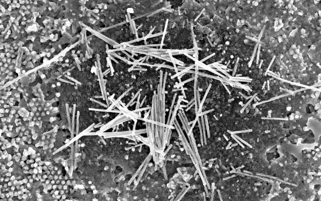
In a recent study, researchers created nanowires made from niobium arsenide, a Weyl semimetal material.
Using a technique called thermomechanical nanomolding, scientists produced single-crystal nanowires measuring only about 40 nanometers wide.
The results were promising.
Researchers found that:
- Smaller nanowires showed lower electrical resistance
- 40 nm wires had significantly improved conductivity
- Surface conduction appeared to be responsible for the improvement
At room temperature, the nanowires demonstrated resistance around 70% lower than bulk single crystals.
Could These Materials Replace Copper?
Although the results are promising, niobium arsenide is not yet ready to replace copper in commercial chips.
Several challenges remain.
Material Limitations
Arsenic is toxic, creating concerns for large-scale manufacturing.
Manufacturing Compatibility
The current fabrication method is not compatible with existing CMOS semiconductor production processes.
Industrial Scaling
Large-scale production of defect-free nanowires remains challenging.
However, researchers believe the discovery proves that topological materials could become realistic engineering solutions rather than only laboratory concepts.
The Future of Semiconductor Interconnects
As artificial intelligence, quantum computing, and high-performance computing continue advancing, semiconductor manufacturers need new materials to overcome physical limits.
Future chip technologies may depend on combinations of:
- Advanced packaging
- New semiconductor materials
- Quantum-inspired electronics
- Three-dimensional chip architectures
Topological semimetals could become part of this next generation of computing infrastructure.
Why This Matters for Future AI Hardware
AI systems require enormous amounts of data movement.
In advanced processors, transferring information between computing units can consume significant energy.
Better interconnect materials could help:
- Reduce power consumption
- Increase processing speed
- Improve thermal performance
- Enable smaller chip designs
The future of AI hardware may depend not only on smarter algorithms, but also on revolutionary materials that allow electrons to move more efficiently.
